How To Read A Timing Diagram
Dram read timing Dram timing sram architecture memory computer write refresh ppt powerpoint presentation slideserve Timing diagrams of 8085
[Solved] Q4-8) Draw a timing diagram for a write operation with no wait
Timing shift I2c protocol timing diagram both interface wire two signal robust concise embedded Dram timing
Have a signal be both robust and concise?
Timing software explainedTiming diagram of inr m Time timing diagram add execution taken graphical represents representation ppt cycle powerpoint presentation slideserveEducation for all: timing diagram for memory write machine cycle.
Timing diagram inr opcode instruction fetch states geeksforgeeks t1 t4Timing q4 science two Timing diagram mvi inr instructions 8085 machine cycle data microprocessor memoryHow to read timing diagrams: a maker’s guide.

This timing diagram explains the operating principle of our 10t sram
Timing diagram basics — rheingold heavyTiming-diagram-of-inr-mvi-instructions 8085 -free 8085 microprocessor Draw timing diagram of memory read and memory write machine cycle inHow to read timing diagrams: a maker’s guide.
[solved] q4-8) draw a timing diagram for a write operation with no waitTiming diagram showing the example task set accodingly to the rm Sram timing 10t principleMaximum timing diagram 8086 mode minimum materials engineering.

Timing mvi machine diagram opcode 45h technobyte
Timing scheduling rmMemory timing fpga diagram blocks least ways set hackaday io Timing diagrams and machine cyclesTiming 8085 microprocessor.
Timing diagram 8085 microprocessorMemory read timing diagram machine cycle Timing diagrams powerpointTiming diagram read mode write memory cycle maximum 8086 draw explain machine.

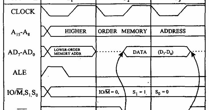
Engineering materials: timing diagram of minimum and maximum mode 8086
Timing diagram describe enoughEducation for all: timing diagram for memory read machine cycle Timing diagram explainedTiming 8085 microprocessor.
Timing memory write diagram machine cycle education fig .


![[Solved] Q4-8) Draw a timing diagram for a write operation with no wait](https://i2.wp.com/www.coursehero.com/qa/attachment/10946523/)


